The automotive industry has a lot of technical progress ahead in the coming years, not least with the rise of electric vehicles. Innovation is one of the keys to Renault Group’s success, with its Technocentre in Guyancourt, one of the largest automotive R&D centers in Europe.
Cars now pack in so many new features that people talk about “smart vehicles”. Gesture recognition, virtual assistants, gaze detection, driver attention monitoring: these functions will build on today’s advances in accident prevention. They are made possible by the development of electronics and the integration of numerous sensors in modern vehicles.
Thanks to CT, understanding failure mechanisms helps guarantee quality levels that hold up in large-scale manufacturing and distribution.
X-ray micro-CT at Renault Group
Failure analysis of electronic parts follows the same approach as for mechanical parts: it always starts with so-called level 1 analyses, using non-destructive means.
For electronic parts, the essential tools are radiography and microfocus X-ray CT. They let us see inside parts and components, locate defects and, where possible, identify failure mechanisms. When it’s permitted, this allows us to move on to more intrusive analyses, targeting the sampling very precisely so that the defects and the signatures of the failure aren’t destroyed.
In today’s electronics world, the challenge is to reach ever smaller defects, which means having tools capable of very high resolutions.Challenges solved with CT
The following analyses were carried out with the nano-CT EasyTom 160 kV system designed by RX Solutions.
Here is one of the challenges we faced, on cracked diodes.
“High-resolution CT scans showed the cracks in the glass unambiguously. A mechanical cross-section wouldn’t have led to a conclusion, because cutting the part could itself have created these cracks in the brittle glass. The cracks are only a few microns wide.”Water sensor: cracked diodes
The sensor is a board encapsulated in black resin. The part was inspected whole, at 100 × 80 × 60 mm.
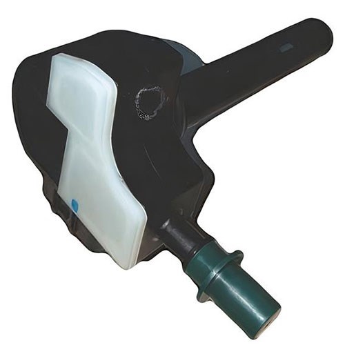
Failure: non-functional sensor.
Analysis challenge: revealing cracks in a very small glassy material within a large part.
Root cause: mechanical breakage of the diodes’ glass due to mechanical stress.
Hypothesis: the mechanical stresses induced by the resin (during curing, for example) may have put the PCB under slight bending because of its design. This would have caused the two diodes located in the area most sensitive to that bending to break.
Positioning the sensor in the CT system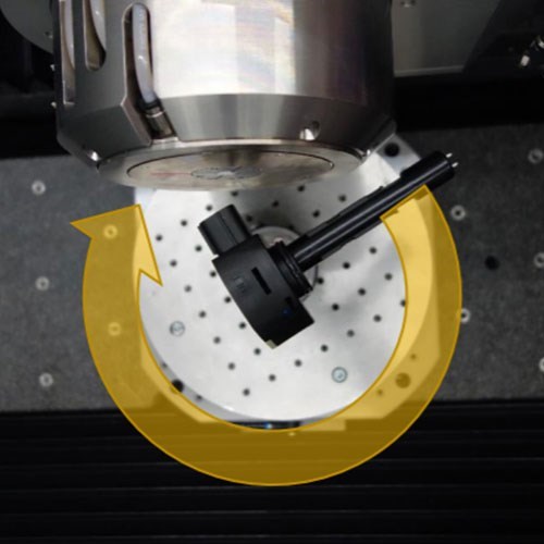 Limited-angle acquisition, giving high magnification despite the part’s 10 cm-long arm
Results from the diode CT scans
Image 1: location of the diodes in question in the water sensor.
Images 2 & 3: cracks in the glass of the diodes.
EasyTom 160 – voxel size: 2 µm.
Whole-part acquisition, 100 × 80 × 60 mmX-ray CT: a key tool for electronic failure analysis
X-ray CT is a powerful technology that can be used for a wide range of applications, from materials analysis to assembly inspection, including dimensional measurements.
For failure analysis of on-board electronics, high-resolution CT lets you inspect internal components without risking further damage to the part under investigation, which could destroy or lose the very elements needed to reach a conclusion.
A system like RX Solutions’ EasyTom makes it easy to work at several scales, moving from an overall view of the component to a targeted, very-high-resolution analysis, even though the part is bulky. That makes it a tool of choice for failure analysis in on-board electronics.
CT & automotive: learn more
Discover battery applications